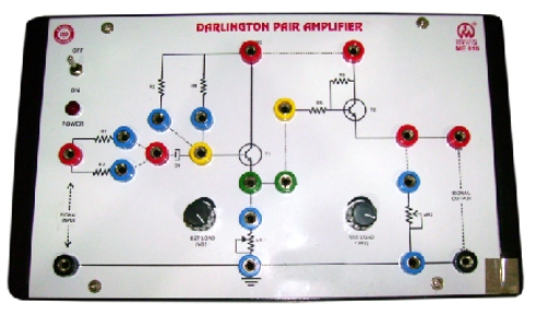
Darlington Pair Amplifier (ME 610)
Darlington Pair Amplifier has been designed to study the following : A. Output Voltage Gain. B. Output Impedance. C. Output Power.
Product Overview
Darlington Pair Amplifier has been designed to study the following : A. Output Voltage Gain. B. Output Impedance. C. Output Power.
Darlington Pair Amplifier has been designed
to study the following :
A. Output Voltage Gain.
B. Output Impedance.
C. Output Power.
Inbuilt Fixed DC Regulated Power Supply
Output Voltages: 12VDC
Transistor , Potentiometer & Components Provided
Transistors: CL100 (NPN) .
Potentiometer: To measure the Input/Output impedance.
For more details please refer datasheet.
Technical Specifications
Darlington Pair Amplifier has been designed
to study the following :
A. Output Voltage Gain.
B. Output Impedance.
C. Output Power.
Inbuilt Fixed DC Regulated Power Supply
Output Voltages: 12VDC
Transistor , Potentiometer & Components Provided
Transistors: CL100 (NPN) .
Potentiometer: To measure the Input/Output impedance.
For more details please refer datasheet.
Talk To Our Technical Experts
Related Products
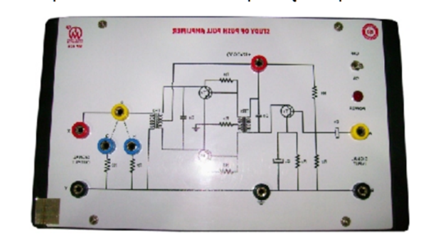
Biasing of Transistor As Class 'A' Amplifier (ME 623)
Biasing of Transistor as Class
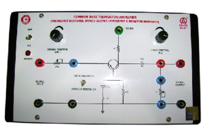
Common Base Transistor Amplifier (ME 617)
Common Base Transistor Amplifier apparatus with and without Negative Feed Back has been designed to study the following :- A. Frequency Response / Output Voltage Gain. B. Input Impedance. C. Output Impedance. D. Effect of Negative Feed Back on Output Gain
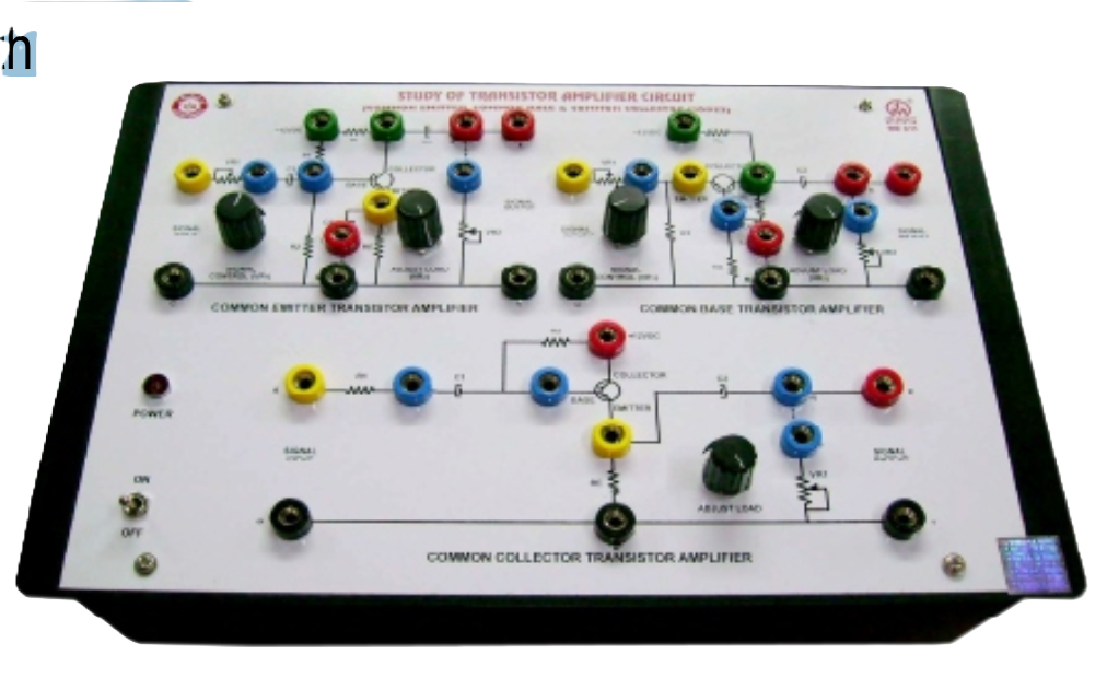
Study of Transistor Amplifier Circuits (With in Common Base, Common Emitter & Common Collector Mode) (ME 611)
Transistor Amplifier Circuits has been designed to plot the frequency response and to measure the following: A. EffectofFeed-Back onoutputinCommonBase&CommonEmitter Amplifier. B. Input Impedance C. Output Impedance D. Band Width E. Gain
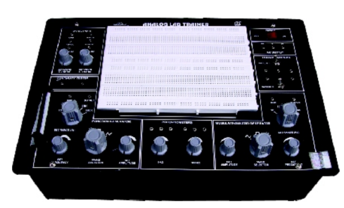
Analog Lab Trainer (Bread Board Model) (ME 1153)
Advanced lab trainer for students to perform more than 50 experiments of analog electronics