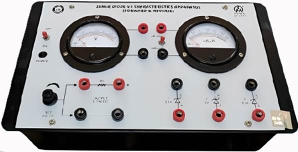
Zener Diode V-I Characteristics Apparatus (ME 542RFD)
Zener Diode V-I Characteristics Apparatus
Product Overview
Zener Diode V-I Characteristics Apparatus
Inbuilt VariableDC Regulated Power Supply
Output voltages : 0-15VDC
On Board Analog Moving Coil Meters (60 mm x 35 mm )
Voltmeter : 0-15VDC
Ammeter : 150MicroADC/15mADC (dual range)
Resistance & Diode provided
Zener Diode : 5.1V, 6V, 8.2V
Symbol diagram printed on Aluminum Front
Panel & all important test Points
For more details please refer datasheet.
Technical Specifications
Inbuilt VariableDC Regulated Power Supply
Output voltages : 0-15VDC
On Board Analog Moving Coil Meters (60 mm x 35 mm )
Voltmeter : 0-15VDC
Ammeter : 150MicroADC/15mADC (dual range)
Resistance & Diode provided
Zener Diode : 5.1V, 6V, 8.2V
Symbol diagram printed on Aluminum Front
Panel & all important test Points
For more details please refer datasheet.
Talk To Our Technical Experts
Related Products
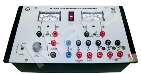
PN/Zener Diode/ LED Characteristics Apparatus (ME543)
Forward and Reverse bias V-I characteristics of PN junction diode, Zener diode& forward bias characteristics of a LED.
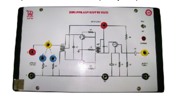
Biasing of Transistor As Class 'A' Amplifier (ME 623)
Biasing of Transistor as Class
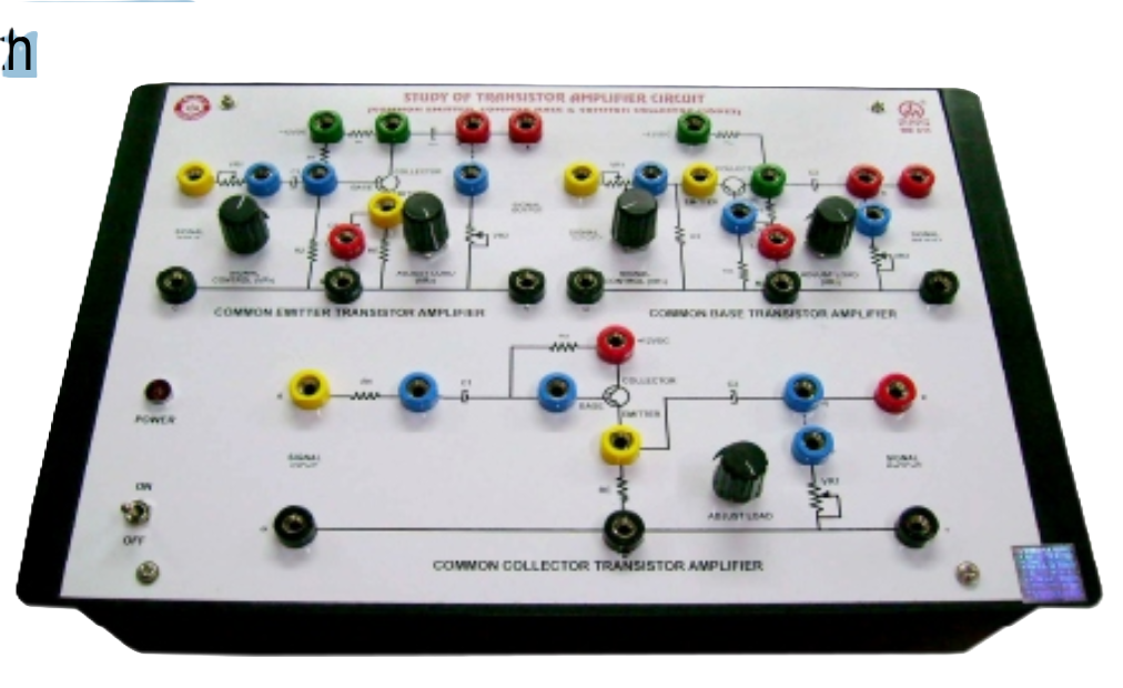
Study of Transistor Amplifier Circuits (With in Common Base, Common Emitter & Common Collector Mode) (ME 611)
Transistor Amplifier Circuits has been designed to plot the frequency response and to measure the following: A. EffectofFeed-Back onoutputinCommonBase&CommonEmitter Amplifier. B. Input Impedance C. Output Impedance D. Band Width E. Gain
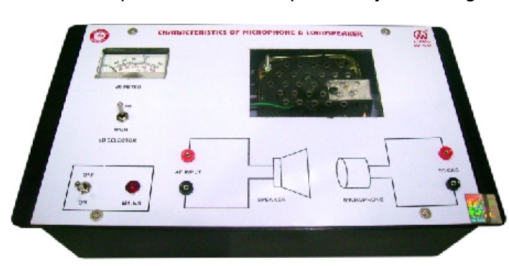
Microphone and Loudspeaker Characteristics Apparatus (ME 536)
Plot frequency response characteristics of Microphone and Loudspeaker